


The increasing use of complex algorithms in embedded control systems is adding substantially to processing overhead. The computational intensity often outstrips the capabilities of standard 32-bit microcontrollers. Since most MCUs are not capable of this level of computation, it is common to use a digital signal processor (DSP) to execute these algorithms, plus then, a microcontroller for the control functions. A major drawback to a two-processor approach is that code must be written separately, increasing the development cycle and failure risk.
To address this issue, several processor vendors have integrated DSP instructions in their embedded controller architectures. These MCU/DSPs provide a single chip solution, in a unified software development environment, that can execute both embedded control functions and DSP computations. In less demanding applications, this offers a suitable solution with very low power consumption. However, as small portable end-products increase in complexity, computational processing increases exponentially. The traditional response is to increase the processor clock, which also increases power consumption - but this is unsuitable for small footprint, battery-powered products.
Atmel's AVR group approached this challenge by developing a new MCU/DSP architecture that executes more DSP operations per clock cycle, so it can achieve the higher computational throughput of next generation applications, with a very low clock frequency and exceptionally low power consumption.
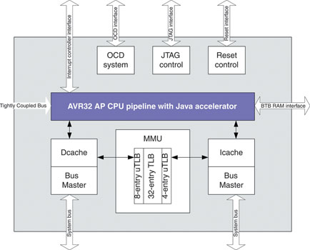
In most RISC architectures many cycles are wasted on power-hungry, non-productive activities such as loading, storing and moving data around, branches, cache misses, and on stalled instructions waiting for the pipeline to execute multicycle operations. None of these activities make a contribution to application execution. In fact, they reduce the execution throughput per cycle. The AVR32 core (Figure 1) achieves higher throughput by eliminating non-productive processor cycles the following: 1) reducing the number of load/store cycles, 2) maximising the utilisation of computational resources, 3) providing zero-penalty branches, and 4) reducing the number of cache 'misses'. In addition, the AVR32 core is architected specifically to minimise both active power consumption and current leakage.
Reducing cycles
On average, 30% of a processor's cycles are spent, not on operations, but on load/store instructions. The AVR32 reduces the required number of load/store instructions with byte (8-bit), half-word (16-bit), word (32-bit) and double word (64-bit) load/store instructions that are combined with various pointer arithmetic to efficiently access tables, data structures and random data in the fewest number of cycles. For example, block cipher algorithms, used in cryptography, require a special array addressing operation with a long instruction sequence, dominated by four memory access operations extracts one of the four bytes in a 32-bit word, zero-extends it and adds it to a base pointer. The result of this operation generates the memory address to be accessed. It can take 14 cycles to execute on a conventional processor.
result = pointer0[offset0 >> 24] ^
pointer1[(offset1 >> 16) & 0xff] ^
pointer2[(offset2 >> 8) & 0xff] ^
pointer3[offset3 & 0xff];
The AVR32 has a novel 'load with extracted index' (ld.w) instruction that reduces this operation to just seven cycles by performing all four memory accesses in four cycles, while keeping all four offsets in one register. Another cycle-saving load/store instruction, 'load multiple register' (ldm), can be used in combination with a 'store multiple' (stm) instruction to fetch two and two registers from the data cache. The instruction can be used to return from the subroutine as the last register written can be the program counter, completely eliminating the need to execute a return instruction at the end of the subroutine. By reducing the number of load/store instructions to be executed, the AVR32 core increases the throughput per cycle. Altogether the AVR32 core has 28 instructions that increase the efficiency of load/store operations.
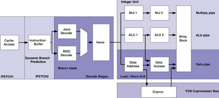
The AVR32 CPU has a 7-stage pipeline with three sub pipelines (multiplication/MAC, load/store, and ALU) that allow arithmetic operations on non-dependent data to be executed, out of order and in parallel (Figure 2). A conventional architecture has a single pipeline that stalls the code until each instruction is completed. This can waste valuable computational resources during multicycle instructions. Logic in the AVR32 pipeline allows non-dependent instructions to be executed simultaneously, using available pipeline resources. Out of order execution can increase the throughput per cycle. Hazard detection logic detects and holds dependent instructions at the beginning of the pipeline until the operation on which they depend is complete.
DSP algorithms consist to a large degree of multiply/accumulate (MAC) operations in which two values are multiplied times each other and repeatedly added to a third value. Processor architectures typically deal with MAC operations by performing the multiplication and then adding the result to a value stored in a register. The number of cycles used for the MAC operation often depend on the number of read and write ports in the register file. Each read and write port is expensive in term of silicon area, but also in power consumption since each register file access toggles a lot of power hungry lines inside the register file RAM. If the multiplier has two read and write ports, this operation will take two cycles, one to perform the multiplication and a second one to perform the addition. Adding another read and another write port makes it possible to execute a MAC in a single cycle. However, the extra ports increase the silicon cost and the power consumption of the CPU. As a result, the chip designers have had to make a trade-off between the silicon cost and power consumption and performance.
Atmel's AVR32 engineers have developed a patented means of executing single-cycle MACs without the penalty of extra ports on the multiplier, by developing a patent-pending 'accumulator cache' inside the multiplier. The accumulator cache is used to store the value that is to be added to. Since MACs always require that the multiplicand be added to the last value, there is no need to use external registers. Thus, the result of the multiplication is added to the value in the cache, and the next result is added to that value, and so on. This allows the MAC operation to be executed in a single cycle using a minimum number of read and write ports and no external registers.
The AVR32 eliminates many of the cycles: used to write to and read from register files by forwarding data between the pipeline stages. Instructions that finish execution before the writeback stage are immediately forwarded to the beginning of the pipelines to be used immediately by the instructions waiting for them. By minimising the number of register file accesses, this feature saves both cycles and power consumption. All AVR32 results are forwarded as soon they are finished.
Single-instruction multiple data (SIMD) instructions in the AVR32 architecture can quadruple the throughput of certain DSP algorithms that require the same operation to be executed on a stream of data (eg, motion estimation for MPEG decoding). An 8-bit sum of absolution differences (SAD) calculation is executed by loading four 8-bit pixels from memory in a single load operation, then executing a packed subtraction of unsigned bytes with saturation, adding together the high and low pair of packed bytes and unpacking them into packed half-words. These are then added together to get the SAD value.
Branch prediction and folding can achieve zero-cycle penalty in loops. Although deep pipelines enable higher clock frequencies, they introduce significant cycle penalties whenever there are jumps in the program flow. These branch penalties are particularly harsh for small inner loops. To address this problem, the AVR32 pipeline has branch prediction logic that can accurately predict all change-of-flow instructions. In addition, branches are 'folded' with the target instruction, resulting in a zero-cycle branch penalty.
The AVR32 instruction set evolved from extensive benchmarking and refinement in cooperation with compiler vendor, IAR. The result is code density that is 10% to 50% more dense than that of ARM9 or ARM11 cores, using the EEMBC benchmark suite. Denser code allows more instructions to be stored in the processor cache, thereby reducing the number of cache misses and increasing overall processor throughput per cycle.
Better performance per MHz
The AVR32's novel instruction set architecture, including load/store instructions with pointer arithmetic, in combination with parallel computational pipelines that allow out-of-order execution, and keep data inside the pipeline by using data forwarding and the accumulator cache all contribute to exceptional computational throughput per clock cycle of the AVR32 core. The EEMBC benchmarks processor performance on a wide range of algorithms, using non-optimised, compiled code. Throughput is measured by number of times each algorithm can be executed per second at a given clock rate. Results will vary, not just based on the processor's efficiency, but also on the data being operated on and on the efficiency of the compiler.
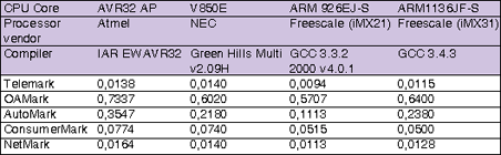
The EEMBC also groups together the algorithms that are frequently used in certain classes of applications (eg, networking, consumer, etc) and takes a geometric mean of the pertinent benchmarks to arrive at a benchmark for that application class (see Table 1). All scores are normalised to the processor running at 1 MHz - they therefore show the architectural throughput of the processor, not the absolute processing performance at speed. The numbers represent a benchmark score, calculated after formulas given by EEMBC, where bigger is better.
The AVR32 architecture is not just about massive amounts of throughput and a high clock rate. It is about providing sufficient processing power with minimal power consumption to handheld, battery operated end-products, such as handheld video players, handheld POS terminals and handheld medical equipment. The superior throughput of the AVR32 core allows a slower clock frequency which provides a linear reduction in power consumption. In addition, the AVR32 is designed to minimise active power consumption at any clock rate by keeping data close to the CPU and minimising the unnecessary movement of data on buses that consume a lot of power.
For example, older MCUs architectures copy the return address of a subroutine call to a memory stack, consuming unnecessary power. The AVR32 eliminates this need by including a link register in the register file. The use of data forwarding and the accumulator cache keep data inside the pipeline, greatly reducing the overall power consumed and limiting the need for power-hogging accesses of registers or external memory stacks. Another power-saving device is to keep the status register and the return address for interrupts and exceptions in system registers, rather than moving data to and from the stack. The high code density of the AVR32 also helps reduce power consumption by reducing the number of cycles and external memory accesses wasted on cache misses.
Next step: SoC-level integration
The primary focus for the development of the AVR32 core was to increase throughput sufficiently to run computationally-intensive applications at a quite slow frequency to save power. Since battery capacity is not keeping up with increased processing requirements, this type of approach is mandatory. Another way to save power is to integrate as many chips as possible on the same piece of silicon. Atmel has taken 2/3 of the chips required in a multimedia system and integrated them on its AP7000 processor to create a true system-on-chip with virtually all the peripherals and interfaces required for target applications.
The AP7000 integrates Atmel's AVR32 MCU/CPU core with a vectored multiplier coprocessor, 32 KB on-chip SRAM, 16 KB instruction and 16 KB data caches, memory management unit, and multiple on-chip DMA controllers. Peripherals include a bit-stream audio DAC, TFT/STN LCD & HDD controllers, 480 Mbps USB 2.0 with on chip transceivers, and two 10/100 Ethernet MACs. Serial interfaces include RS232, USART, I2S, AC97, TWI/I2C, SPI, PS/2 and several synchronous serial modules (SSC) supporting most serial communication protocols. In many applications, the AP7000 is a single-chip solution, with substantially less capacitance than a discrete solution.
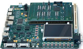
An AP7000 development kit (Figure 3) is available that consists of a true single-board computer with the AP7000 processor, LCD display, Dual Ethernet ports, USB Device and Host-ports, PS2 ports, UARTs and connectors for all on-chip peripherals on the AP7000.
AP7000 software is developed and debugged in a single, MCU-style development environment. SIMD- and DSP-aware compilers are available from Atmel (GNU GCC) and IAR Systems (Embedded Workbench). The AP7000 has a fully supported Linux 2.6 kernel to support open source code.
| Tel: | +27 11 923 9600 |
| Fax: | +27 11 923 9884 |
| Email: | [email protected] |
| www: | www.altronarrow.com |
| Articles: | More information and articles about Altron Arrow |
| Tel: | +27 11 236 1900 |
| Fax: | +27 11 236 1913 |
| Email: | [email protected] |
| www: | www.ebv.com |
| Articles: | More information and articles about EBV Electrolink |


© Technews Publishing (Pty) Ltd | All Rights Reserved
 printer friendly version