


Ref: z2717156m
Demanding requirements are placed on high-performance analog-to-digital converters (ADCs) and analog components in most digital receivers. In cellular base station digital receivers for example, sufficient dynamic range is needed to handle high-level interferers (or blockers) while properly demodulating the lower level desired signal.
Maxim's MAX1418 15-bit 65 Msps or MAX1211 12-bit 65 Msps ADC in combination with the MAX9993 2 GHz or MAX9982 900 MHz integrated mixers provides exceptional dynamic range for two of the most critical stages in a receiver line-up. In addition, Maxim's MAX2027 and the MAX2055 IF digital variable gain amplifiers (DVGAs) provide exceptionally high third order output intercept performance (OIP3) with the required gain adjustment range for many applications.
A cellular base station (BTS: base transceiver station) consists of many different hardware modules including one that performs the RF receiver (Rx) and transmitter (Tx) functionality - namely a transceiver (TRx). In the older analog AMPS and TACS BTSs, one transceiver handles a duplexed Rx and Tx RF carrier. Many transceivers are needed to provide enough carriers to obtain the required calling coverage.
Analog technology is being replaced by CDMA and WCDMA worldwide, and Europe adapted GSM over a decade ago. In CDMA, many callers use the same RF frequency, which allows a single transceiver to handle many callers' signals simultaneously. Various CDMA and GSM designs exist today and methods to reduce cost and power are continuously being sought by BTS manufacturers. Optimising single-carrier solutions or developing multicarrier receivers can accomplish this.
Figure 1 illustrates the main blocks in a subsampling receiver architecture commonly used in BTS equipment.
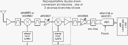
Maxim's MAX9993 2 GHz mixer and MAX9982 900 MHz mixer provide the gain and high linearity coupled with low noise figure allowing the designer to eliminate lossy, passive mixers in many designs. The MAX2027 and MAX2055 are designed to operate in the first or second IF stages of the receiver. Both offer +40 dBm third order output intercept (OIP3) performance over their entire gain adjustment range. Even though the MAX1418 (15-bit 65 Msps) and MAX1211 (12-bit 65 Msps) data converters are illustrated in Figure 1, other speed grades satisfying most applications are included in both converter families. If the second down conversion is eliminated (shown in dashed lines), the figure depicts a single down conversion architecture.
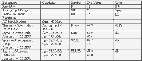
Maxim's low noise ADC, MAX1418: For the subsampling receiver architecture shown in Figure 1, stringent noise and distortion requirements are placed on the ADC. In receiver applications, the lower level desired signal is digitised alone or in the presence of an unwanted signal(s) that can be significantly larger in amplitude. To properly design the receiver, the ADC effective noise figure must be determined under these two signal extremes. The converter's noise figure is determined by comparing its total noise power to the thermal noise floor. For small analog input signals, the thermal + quantisation noise power dominate the ADC's noise floor, which is used to approximate the ADC's effective noise figure (NF).
In practice, once the ADC's effective noise figure is known in the small signal condition, and the cascaded noise figure of the analog circuitry (RF and IF) is determined, the minimum power gain ahead of the ADC is selected to meet the required receiver noise figure. The amount of power gain places an upper limit on the maximum blocker, or highest interference level the receiver can tolerate before the ADC overloads. For BTS applications, the ADC often does not have sufficient dynamic range to meet both the noise figure requirements (receiver sensitivity) and maximum blocker requirements without implementing automatic gain control (AGC). The AGC can be included either in the RF stages, IF stages, or both.
Other converters in the MAX1418 family are optimised for baseband performance where fINPUT<fCLOCK/2. Operating in this frequency range and using these baseband optimised parts provide the best possible converter dynamic range. These converters include the MAX1419 optimised for a 65 Msps clock rate and the MAX1427 optimised for a clock rate of 80 Msps, both with SFDR performance equal to 94,5dBc at baseband.
The following example uses the MAX1418 specifications listed in Table 1:
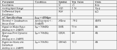
The MAX1418 can be used with a 14-bit interface by not connecting the LSB. If so used, there is a slight SNR performance penalty and the SFDR performance remains essentially unaffected.
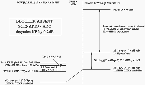
Figure 2 illustrates the ADC noise contribution in the absence of a large-level blocker. Assume all the analog circuitry in front of the ADC has a cascaded noise figure of 3,5 dB. As a first approximation, suppose a designer's goal is for the ADC to degrade the overall receiver noise figure by no more than 0,2 dB to meet some target sensitivity in a CDMA base station receiver. This noise figure value should provide sufficient margin to the air-interface requirements, which is also dependent on the final detector's Eb/No (bit energy to noise power spectral density ratio) requirement. If the MAX1418 thermal + quantisation noise floor value from Table 1 is used, an equivalent noise figure of 26,9 dB can be calculated when the device is clocked at 61,44 Msps (50x chip rate). The ADC noise in the 1,23 MHz CDMA channel bandwidth is 14 dB lower than the noise in the Nyquist bandwidth due to the processing gain achieved. An overall gain of 36 dB is needed to achieve the desired cascaded receiver noise figure value of 3,7 dB.
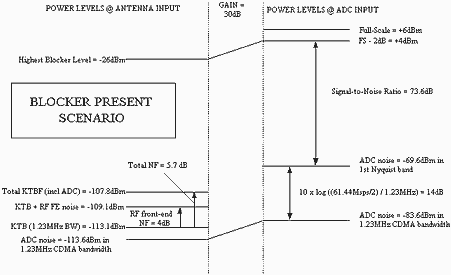
With 36 dB gain ahead of the ADC, a maximum single tone blocker level above -30 dBm at the antenna terminal will exceed the ADC full-scale input. The cdma2000 cellular base station standard specifies a maximum allowable blocker level of -30 dBm at the antenna terminal. For this example, 6 dB gain reduction is used to increase the largest allowable blocker signal applied to the ADC providing margin to the standard's specification. Assuming 2 dB headroom is allowed, 6dB gain reduction results in a maximum blocker level of -26 dBm at the antenna and +4 dBm at the ADC input (see Figure 3). The cellular standards allow 3 dB degradation in overall (noise + distortion) relative to reference sensitivity when a single-tone blocker is present. The allocation of individual noise and distortion components is left up to the designer.
Suppose the designer allows the RF front-end cascaded noise plus distortion to degrade the NF by 1 dB (from the nominal 3,5 dB) when the blocker is present with 6 dB of AGC applied. With only 30 dB of gain in front of the ADC and an effective noise figure of 29,4 dB determined by the ADC SNR performance, the cascaded receiver noise figure is 5,7 dB in the 'blocked condition', which is a 2 dB degradation from 3,7 dB noise figure calculated for receiver sensitivity. Because this calculation does not take into account the spurious performance, an additional 1 dB degradation can be allowed for the ADC's spurious free dynamic range (SFDR) performance. Instead of calculating noise and SFDR contributions separately, SINAD could have been used to compute the effective NF when a blocker signal is present.
MAX1211 allows single down conversion architecture: The subsampling architecture can be used with a single down conversion architecture if sufficient SNR and SFDR performance can be obtained from the converter at higher IF frequencies. Maxim's MAX1211 is a 12-bit 65 Msps converter designed with this architecture in mind along with pin-compatible 80 Msps and 95 Msps versions that will soon be released. This family of converters allows direct IF sampling for input frequencies up to 400 MHz along with advanced features such as differential or single-ended clock input, allows 20% to 80% clock duty cycle, data valid indicator allowing the simplification of clock and data timing, 2's complement or gray code digital output data format all in a small 40-pin thin QFN package (6 x 6 x 0,8 mm). See Table 2 for the MAX1211 AC specifications illustrating the superior AC performance for an analog input frequency of 175 MHz.
There are significant advantages gained when choosing single down conversion instead of double down conversion. By eliminating the second down conversion mixer, second-IF gain stages, and second LO synthesizer circuitry, the parts count and board space can be reduced by approximately 10% and cost by $10 to $20.
Spurious considerations for different architectures
If saving parts count, board space, power, and cost do not provide enough incentive, the following example illustrates the frequency planning advantage gained when using the MAX1211 in a single down conversion architecture.
Suppose a cdma2000 receiver is designed to operate in the PCS frequency band. For a sample rate of 61,44 Msps and synthesizer reference frequency of 30,72 MHz, choose a first IF frequency centred in the sixth Nyquist band at 169 MHz having a bandwidth of approximately 1,24 MHz. Using the same first IF centre frequency of 169 MHz, the DDC architecture assumes a second IF frequency is centred in the second Nyquist band at 46,08 MHz.
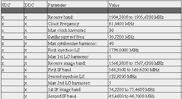
Table 3 lists the spur search assumptions for an RF carrier near the upper end of the PCS band for the single-carrier, single down conversion (SDC) and double down conversion (DDC) architectures. For the SDC architecture, the spur search resulted in 134 total spurs in the RF receive band, receive image band, IF band, and IF image band. Most of these spurs are high order and will not degrade the receiver's performance. For the DDC architecture, this spur search results in over 2400 spurs, which 18 times more than what was calculated for the SDC architecture. These spurious products occur in the RF receive band, receive image band, first IF band, first IF image band, second IF band, and second IF image band. The spurs resulting from combinations of higher clock harmonics and synthesizer reference frequency will be relatively easy to reduce through good board layout practices and filtering. However, a significant number of lower order spurs will be difficult to minimise.
The MAX2027 & MAX2055 IF amplifiers
Maxim also offers high performance IF amplifiers having digital variable gain control in 1 dB increments. The MAX2027 is a digital variable gain amplifier (DVGA) having single-ended input/single-ended output for frequencies ranging from 50 MHz to 400 MHz. This DVGA offers a low noise figure of 5dB at maximum gain. The MAX2055 is a single-ended input/differential output DVGA meant to drive high-performance ADCs for frequencies ranging from 30 MHz to 300 MHz. A step-up transformer can be used between the differential output of the MAX2055 and the ADC differential input. The transformer is driven differentially; thus optimising the transformer performance and balance between the output signals. Both DVGAs operate from 5V bias and have +40 dBm OIP3 over all gain setting ranges. See the associated data sheets on Maxim's web site.
The MAX9993 & MAX9982 high linearity mixers
In receiver circuits, mixers are subjected to large input signals that place stringent requirements on their performance. Ideally, the mixer output signal amplitude and phase are proportional to the input signal's amplitude and phase and independent of the LO signal characteristics. Using this assumption, the amplitude response of the mixer is linear for the RF input and is independent of the LO input.
However, mixer nonlinearities produce undesired mixing products called spurious responses, which are caused by undesired signals reaching the mixer's RF input port and producing a response at the IF frequency. When they interfere with the desired IF frequency, the mixing mechanism can be described by:
FIF = ±m fRF ±n fLO where IF, RF, and LO refer to the signals at designated ports respectively and m and n are integer harmonics of both the RF and LO frequencies that mix to create numerous combinations of spurious products.
Integrated (or active) balanced mixer designs, such as Maxim's MAX9993 and MAX9982 are becoming more popular as their performance rivals that of passive mixer solutions. Balanced mixers reject certain spurious responses when m or n is even resulting in excellent second order harmonic performance. Ideal double balanced mixers reject all responses where m or n (or both) is even. The IF, RF, and LO ports are mutually isolated in all double balanced mixers. With properly designed baluns, these mixers can have overlapping RF, IF, and LO bands.
The MAX9993 and MAX9982 features include: gain, low noise figure, integrated LO buffer, low LO drive, LO switch allowing two LO frequency inputs, superb LO noise performance, and integrated RF baluns on the RF and LO ports.
Maxim's mixers have built-in LO buffers with superior LO noise performance that ease the input LO power requirements driving them. LO noise reciprocally mixes with high-level input blocking signals that desensitise the receiver. Both MAX9993 and MAX9982 have low noise LO buffers designed to have minimal impact on receiver desensitisation when blockers are present. For example, suppose the VCO providing the injection signal has a sideband noise performance of
-145 dBc/Hz. The typical LO noise performance for the MAX9993 is -164 dBc/Hz, so the composite sideband noise performance is degraded by only 0,05 dBc/Hz to -144,95 dBc/Hz. This way, the user not only benefits from needing to provide a low-level LO injection signal to the mixer, but can also be assured the reciprocal mixing performance of the receiver is not degraded due to the MAX9993 LO buffer performance.
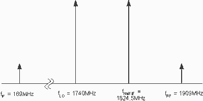
A particularly troublesome second order spurious response called the half-IF (½ IF) spurious response is defined for the mixer indices of (m = 2, n = -2) for low-side injection and (m = -2, n = 2) for high-side injection. For low-side injection, the input frequency that creates the half-IF spurious response is located below the desired RF frequency by an amount fIF/2 from the desired RF input frequency (see Figure 4). The desired RF frequency is represented by 1909 MHz, and in combination with the LO frequency of 1740 MHz, the resulting IF frequency is 169 MHz. Though the CDMA RF and IF carrier occupies a 1,24 MHz bandwidth, it is illustrated as a single frequency indicating the centre carrier frequency.
For this example, the undesired signal at 1824,5 MHz causes a half-IF spurious product at 169 MHz.
Verify:
2 x fHalf-IF - 2 x fLO =
2 x (fRF - fIF/2) - 2 x (fRF - fIF) =
2 x fRF - 2 x fIF/2 - 2 x fRF + 2 x fIF = fIF
Results in:
2 x 1824,5 MHz - 2 x 1740 MHz = 169 MHz
The amount of rejection, called the 2x2 spurious response, can be predicted from the mixer's second order intercept point, IP2. The 2x2 IMR or spurious values in Figure 5 are taken from Maxim's MAX9993 data sheet. Note the signal levels in the figure are referred to the input of the mixer for which the input IP2 (IIP2) performance is calculated.
Such superior level of 2x2 performance results in the following:
IIP2 = 2 x IMR + PSPUR = IMR + PRF
= 2 x 70 dBc + (-75 dBm) = 70 dBc + (-5 dBm)
= +65 dBm
Similarly, Maxim's MAX9982 900 MHz active mixer provides typical 2RF - 2LO spurious response equal to 65 dBc under similar conditions which results in:
IIP2 = 2 x IMR + PSPUR = IMR + PRF
= 2 x 65 dBc + (-70 dBm) = 65 dBc + (-5 dBm)
= +60 dBm
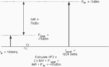
Image-reject filters used in the RF path immediately ahead of the mixer attenuate any amplifier harmonics. The noise filter in the LO path attenuates harmonics caused by the LO injection source. High-level input signals create distortion or intermodulation products and can be quantified by calculating the intercept point, either at the input or output of the device or system. For the case where the mixer LO power is held constant, the order of the intercept point or distortion product is determined only by the RF multiplier and not by the LO multiplier because variations in the RF signal are only of concern. The order refers to how fast the amplitudes of the distortion products increase with a rise in input level.
It has been shown that Maxim's MAX1418 15-bit ADC offers excellent noise performance resulting in low required receiver gain thus withstanding higher blocker or interference levels with minimum AGC. The MAX1211 ADC family is ideally suited for a single-conversion receiver architecture with first IF input frequencies up to 400 MHz. In addition, Maxim's RF MAX9993 and MAX9982 mixers provide the desired linearity along with low noise figure and sufficient power gain to eliminate the need for passive mixers in many of today's receiver designs. Maxim's MAX2027 and MAX2055 DVGAs provide a typical OIP3 value of approximately +40 dBm over their entire gain adjustment range. Taken together, a receiver lineup incorporating these components can achieve a high level of performance in a very cost effective solution.
For more information contact Gareth Kneale, CST Electronics, 011 452 0706.
| Tel: | +27 11 608 0070 |
| Fax: | +27 11 608 0401 |
| Email: | [email protected] |
| www: | www.cstelectronics.co.za |
| Articles: | More information and articles about CST Electronics |


© Technews Publishing (Pty) Ltd | All Rights Reserved
 printer friendly version